Main page
AlterPCB is an open-source, cross-platform PCB design program. It is not meant to be an open-source clone of traditional PCB design software such as Altium or Eagle - if that's what you're looking for, take a look at KiCad. AlterPCB is designed to enable the things that other tools won't allow you to do, because it doesn't fit their design flow. It behaves less like an EDA tool and more like a drawing program for Gerber files. You can draw arbitrary shapes on any layer you want, there are no artificial limitations. This is particularly useful for PCBs that require weird shapes, such as RF filters, antennas, couplers, fanouts for chip-on-board assembly, really dense BGA fanouts, or just PCBs that are meant to be not only functional but also aesthetically pleasing (such as when your PCB doubles as a front panel).
AlterPCB is still under development. There is currently a 'prototype' version written in Python, which is technically usable, but absolutely not user-friendly, and usually too slow for complex designs. The 'real' version is being written in C++, but at this stage it isn't able to do anything useful (we are using a bottom-up approach, so although a lot of low-level work is already done, you can't actually see any of this).
Although it is far from ideal, the Python prototype has been used to successfully create several PCBs, some of which were quite complex.
Examples of PCBs created with AlterPCB
|
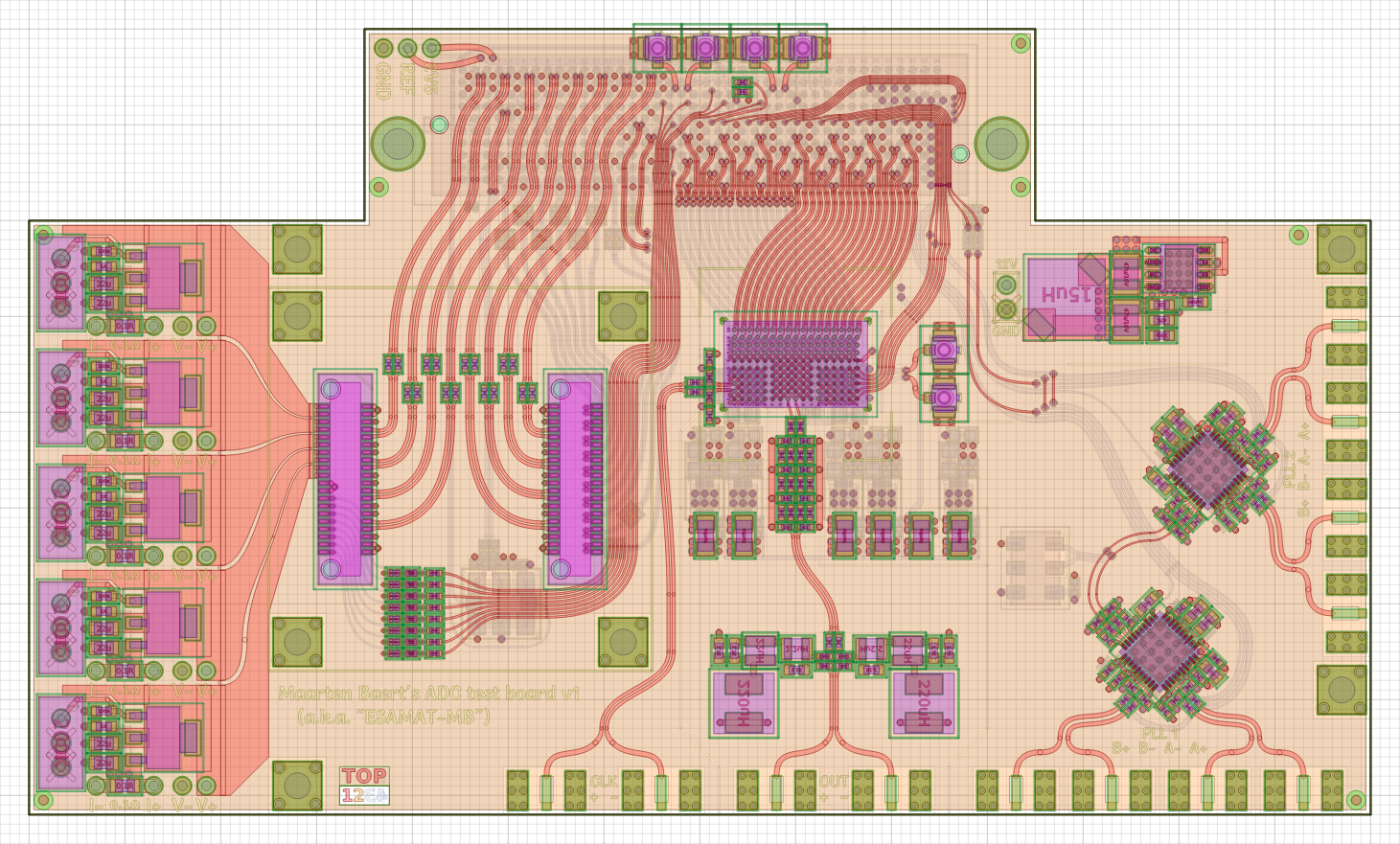
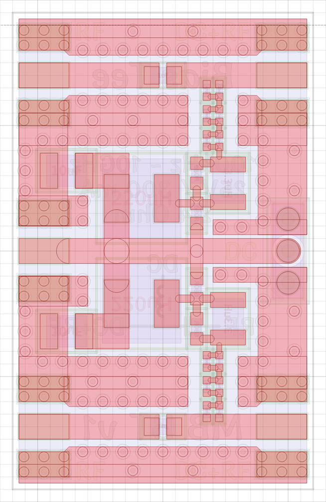
A test PCB with various high-frequency chips and connectors (and several voltage regulators). The 8 wider transmission lines in the upper-left area carry 10 Gbps signals. |
|
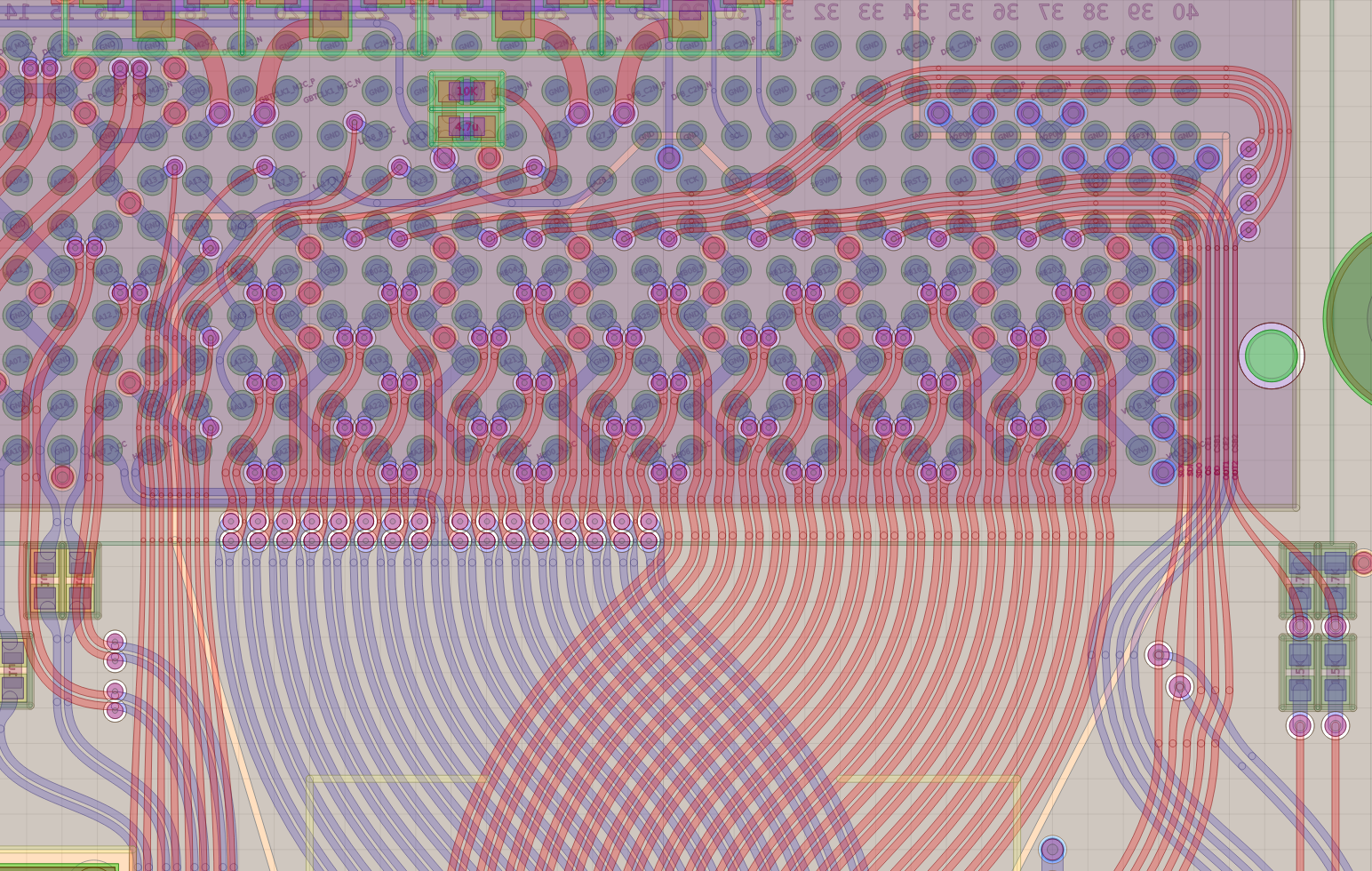
Detail of the FMC connector area. The 34 differential pairs carry 1.25 Gbps LVDS signals, so it was important to maintain the correct characteristic impedance. |
Note that the PCB shown above is far too complex to be edited at a reasonable speed with the Python prototype. During editing, I had to split it up into multiple sub-layouts and use a much lower display quality than what you see in the screenshots. This should no longer be an issue with the C++ version, once it is finished.
Below you can see a demonstration of the different viewing modes. I usually switch between these modes a lot depending on what I'm trying to draw.
|
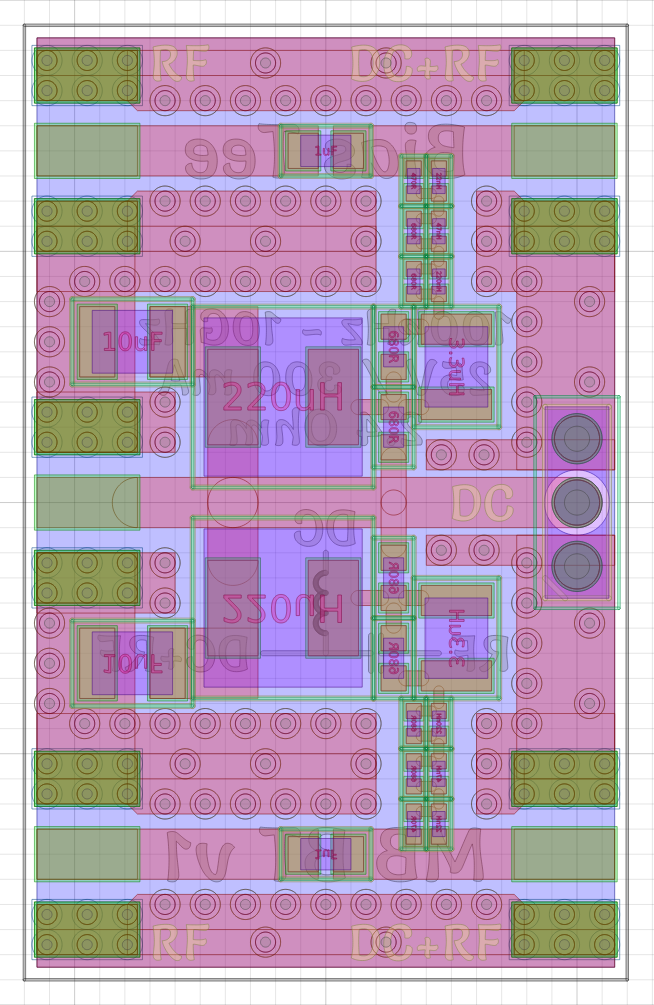
Matched differential bias tee, 'all layer' mode. |
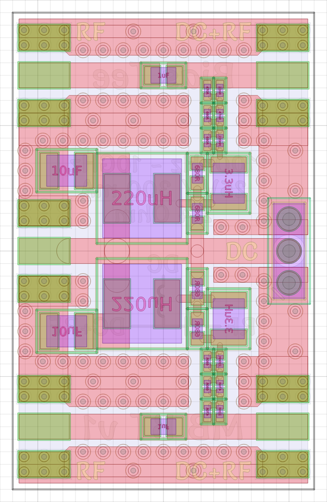
Matched differential bias tee, 'half layer' mode. |
Matched differential bias tee, 'single layer' mode. |
Source code
The C++ version can be found here:
https://github.com/MaartenBaert/alterpcb
Again, this version is still under development and currently not usable.
The Python prototype can be found here:
https://github.com/MaartenBaert/alterpcb-python-prototype
Usable, but very slow and not user-friendly. Incorrect use can produce errors, I have no intention to fix this since this was only a prototype. I do not offer any support for this. Please do not e-mail me questions, bug reports or feature requests, they will probably be ignored.