Triple Feed Patch Array antenna
The Triple Feed Patch Array antenna is a directional circularly polarized antenna based on the original Triple Feed Patch antenna. It uses an array of seven coupled patches, resulting in significantly higher gain. This antenna is not recommended for general FPV use since the beam width is rather narrow, but it should perform very well for long-range flying.
Main features:
-
Good radiation efficiency. Most FR4-based patches have terrible efficiency because FR4 is very lossy at 5.8 GHz. Additionally, most array antennas have higher losses in the feed network. This design uses coupled patches to keep the feed network simple and reduce these losses.
-
Exceptionally good axial ratio, not just directly perpendicular to the patch but also off-center.
-
High gain, though not as high as the theoretical gain of an array with 7 elements. This is because maximizing the gain would result in high sidelobes and a poor axial ratio.
-
Very low sidelobes, almost all energy is concentrated in the main lobe. This increases the width of the main lobe, at the expense of some gain.
-
Reasonably cheap and easy to manufacture with high accuracy, even for a hobbyist.
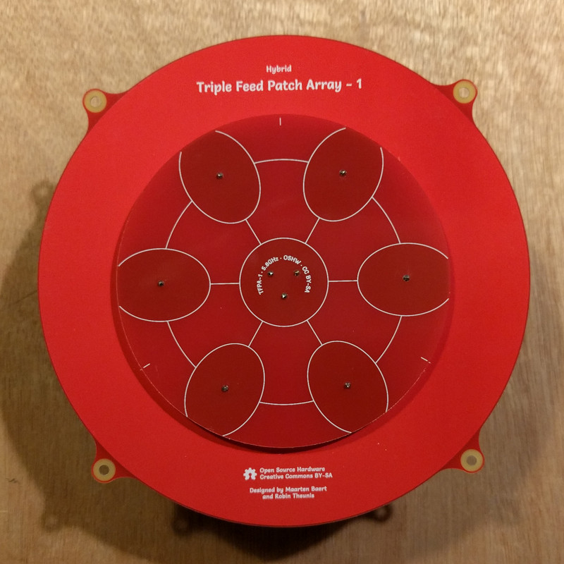
Photo of a Triple Feed Patch Array 1 prototype.
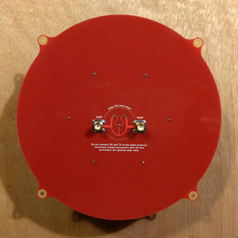
Photo of the back side. This is the 'hybrid' variant, which is simultaneously LHCP and RHCP, with a different connector for each polarization. There is a regular single-connector LHCP/RHCP variant as well.
The photos above show a prototype, the latest design files have an additional copper plane on the back. This copper plane doesn't have any function, but it helps to balance the amount of copper on the top and bottom side of the PCB, which should reduce warping.
Special thanks to Antenna Test Lab who were kind enough to provide complete spherical anechoic chamber measurements (i.e. 3D radiation patterns) for the Triple Feed Patch Array antenna. You can find a detailed test report of the Triple Feed Patch Array antenna on their website.
Specifications
|
Simulated |
Measured |
Notes | |
|
Center frequency |
5.8 GHz |
5.8 GHz ± 100 MHz |
|
|
Bandwidth |
660 MHz (5.47 – 6.13 GHz) |
950 MHz ± 100 MHz |
Feed network losses increase bandwidth |
|
Matching |
S11 < -30 dB, VSWR < 1.065 |
S11 < -20 dB, VSWR < 1.22 |
At center frequency |
|
Axial ratio |
1.05 (0.38 dB) |
1.10 (0.83 dB) |
Averaged over beam width |
|
Antenna gain |
14.4 dBi |
14.0 dBi |
|
|
Half power beam width |
30° |
30° |
Horizontal and vertical |
|
Radiation efficiency |
75% |
74% |
The center frequency may shift a bit between batches as a result of variations in the dielectric constant of FR4. Also, not all brands of FR4 have the same dielectric constant. Frequency shifts up to 100 MHz are normal.
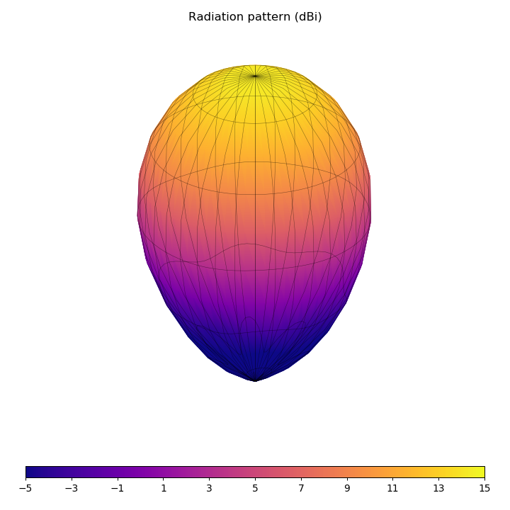
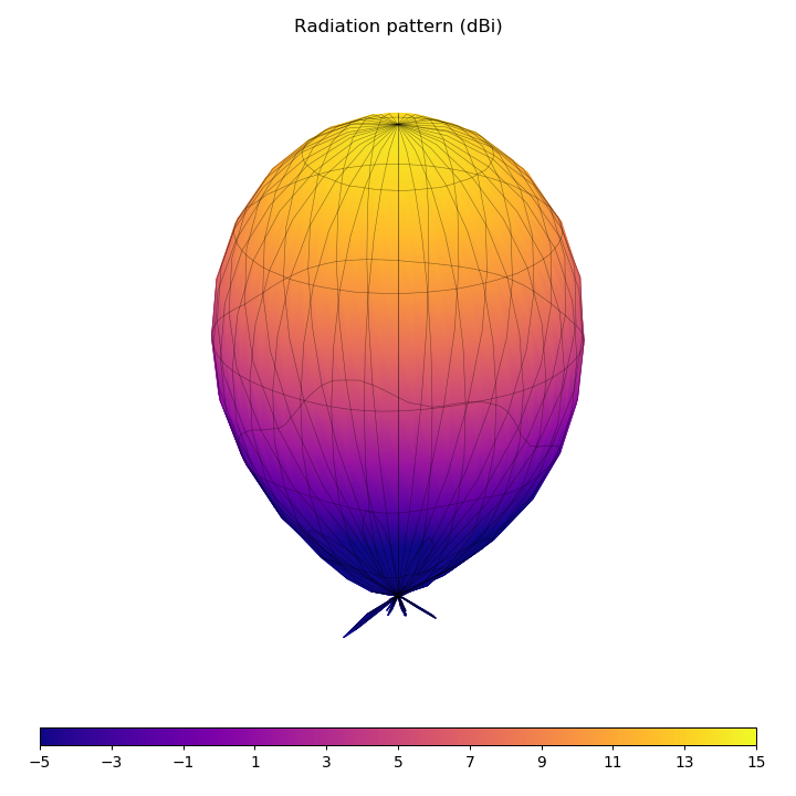
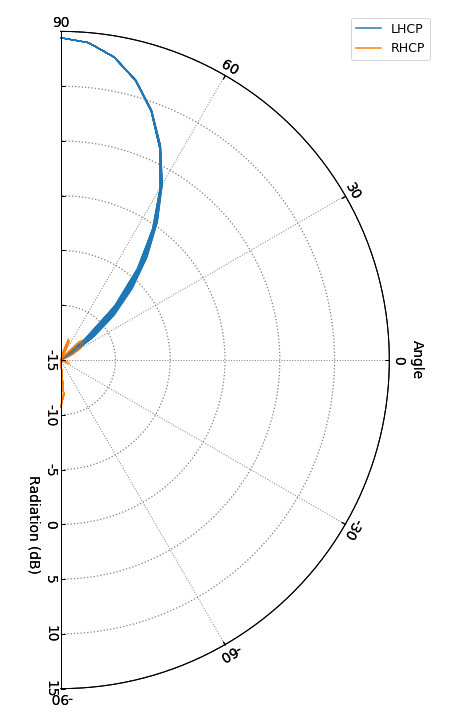
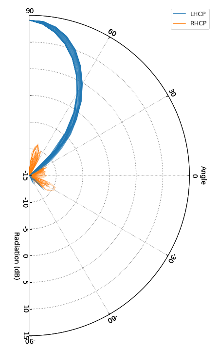
Radiation pattern
|
Simulated (HFSS) |
Measured (anechoic chamber, averaged over full bandwidth) |
|
Simulated 3D radiation pattern. |
Measured 3D radiation pattern, by Antenna Test Lab. |
|
Simulated vertical cross-sections. |
Measured vertical cross-sections, by Antenna Test Lab. |
Note: You are free to use these images for marketing purposes if you are selling Triple Feed Patch Array antennas as long as you link back to this page. Additionally, if you use the images based on the anechoic chamber measurements from Antenna Test Lab, please link back to antennatestlab.com as well.
Animated 3D radiation pattern, by Antenna Test Lab.
VNA measurements
|
VNA measurements (S-parameters). S11 and S22 indicate the reflected power at port 1 and 2 respectively. S12 and S21 indicate how much power is leaking from one port to the other. |
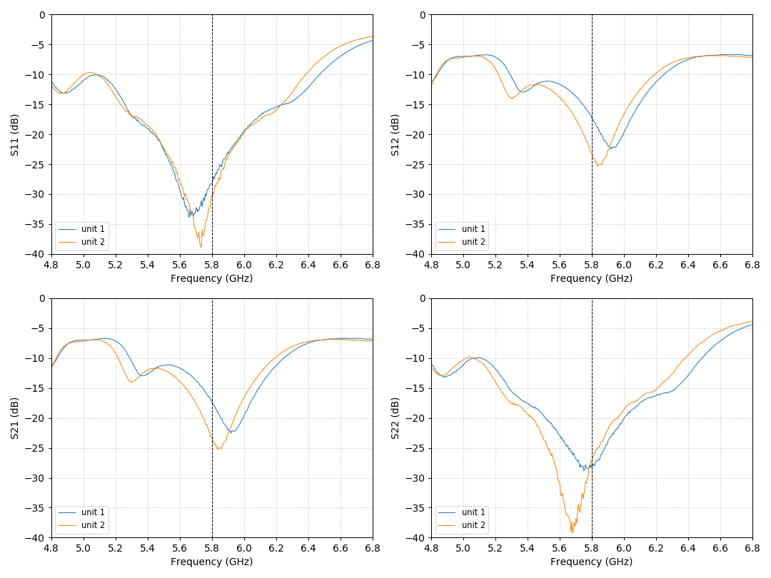
This gives you an idea of the kind of variations you can expect for hand-assembled antennas. Some of the variation is probably caused by the surface-mount SMA connectors since those were soldered by hand, and it's difficult to accurately control the amount of solder when you can't even see the center pin. This affects mostly S11 and S22. The rest is probably the result of inconsistent spacing between the two PCBs, which creates a shift in center frequency. This is clearly visible in S12 and S21. The prototype PCBs were a bit warped which made it difficult to get the correct spacing.
Where can I buy one?
I have no plans to manufacture these antennas myself, I'm hoping that other antenna builders will pick up this design and start selling it.
The following manufacturers are selling the Triple Feed Patch antenna:
|
Manufacturer |
Price* (USD) |
LHCP |
RHCP |
Hybrid |
SMA male |
SMA female |
RP-SMA male |
RP-SMA female |
Notes |
|
$26.77 |
|
|
|
|
|
|
|


* Based on listed price and exchange rate at time of writing. May be outdated. Shipping not included.
If you are a manufacturer who is selling this design, feel free to email me or leave a comment below.
You can also just build them yourself, it's really not that hard. Just download the design files and follow the instructions below.
License

This work is licensed under a Creative Commons Attribution-ShareAlike 4.0 International License.
This means you are free to use this design in any way you like (this includes commercial use) as long as you credit us (Maarten Baert and Robin Theunis). If you choose to modify the design files, you should share the modified design files under the same license.
Design files
Download Triple Feed Patch Array 1 design files (includes LHCP, RHCP and hybrid variant)
Important: This antenna will only work properly when manufactured and assembled correctly. This is not just a regular circuit board, read the instructions below!
Important: If you use Elecrow to manufacture these PCBs, you should add the following note to your order to let them know that the screw holes must be unplated:
The second PCB (pcb_tfpa_1_part2_*.zip) has a separate file for non-plated-through holes (pcb_tfpa_1_part2_*-npth.txt).
Parts
If you decide to build this antenna, you will need the following parts:
-
PCBs: Manufacturers will make these for you if you send them the Gerber files which are included in the design files above. I used Elecrow for my prototypes. Due to the larger size, these PCBs are quite a bit more expensive: the small one costs only $5 for 10 pieces, the large one costs $40 for 10 pieces. That means you end up paying $4.5 per antenna (it gets much cheaper if you make them in larger quantities). The PCBs must use 1.0 mm thickness FR4 material, not the regular 1.6 mm thickness. The correct thickness is critical, if you get this wrong the design won't work properly at all! Regarding copper thickness, 35 µm (1 oz) is fine. Thicker copper tracks won't improve the efficiency at RF frequencies due to the skin effect. The design is tuned for standard FR4, but there may be small variations between different FR4 manufacturers which can result in a shift in the center frequency of the antenna. I specifically made sure that the design isn't too sensitive to material variations, so this shouldn't be a huge problem, but you should still avoid manufacturers that use special materials with different dielectric constants than regular FR4.
-
Copper wire: Regular copper wire with a 1.0 mm diameter is used to create the three feed pins and six support pins. Tin-plated copper or similar is also fine, but don't use iron or steel wire.
-
SMA connector (vertical type): For performance reasons I used surface-mount vertical SMA connectors. I used this for my prototypes. They cost $8 for 10 pieces, so that's $1.6 per antenna. Soldering these requires a hot air rework station or reflow oven, because you can't reach the center pin with a regular soldering iron. Edge-mount connectors are not practical for this antenna, because the long tracks over FR4 would introduce too much loss.
Assembly
The PCBs need to be spaced accurately to get good results. The correct spacing is 3 mm (not 4 mm like the regular Triple Feed Patch). You can buy metal spacers of this height to make this easier. Ideally you need to get these distances right within a 0.1 mm tolerance.
I will add more detailed instructions when I have more time. If you're wondering how you are supposed to solder the center pin of the SMA connectors, there are two ways: pre-tin both the pad and the pin, or use solder paste (I prefer the first option). Place the connector on top of the PCB, and heat it up with a hot air rework station until they join. Adding flux helps. Use tweezers to align the connector properly if necessary. Finally use a regular soldering iron to solder the large ground pad to the connector.
Comments
Tagada73 |
Comment #1: Sun, 13 May 2018, 20:14 (GMT+1, DST) Hi Mr Baert what diameter of your new feed patches? Thanks in advance |
Blackbox |
Comment #2: Thu, 17 May 2018, 18:01 (GMT+1, DST) Hi, thanks for the numerous designs you keep publishing. They really bring the cost of directional antennas down for hobbyists. I have a few questions though. |
Maarten BaertAdministrator |
Comment #3: Thu, 17 May 2018, 21:13 (GMT+1, DST) Quote: Tagada73
Hi Mr Baert what diameter of your new feed patches? Thanks in advance The diameter is 15 cm. Quote: Blackbox
Hi, thanks for the numerous designs you keep publishing. They really bring the cost of directional antennas down for hobbyists. I have a few questions though. The holes have no significant impact on the performance, you can change them or even remove them entirely. If you don't mention that they are unplated, two things can happen: either the manufacturer tries to plate them anyway (very unlikely because there is no copper on the top or bottom), or the manufacturer ignores the file with unplated holes (so there will be no mounting holes). The copper wire diameter is important, you should buy 1mm wire or something very close to it if you don't have it already. Don't try it with e.g. 0.5mm, this will most likely create a significant shift in center frequency and affect the matching between the feed network and the antenna (which can affect the axial ratio). |
Actuna |
Comment #4: Thu, 21 Jun 2018, 20:25 (GMT+1, DST) Hello ... I would like to inform you about the production and sale of the Triple Feed Patch Array (hybrid): Manufacturer: ACTUNA URL: https://actuna.com/Antenna-Triple-Feed-Patch-Array-TFP-A-p22197 Price: 26,32 $ - hybrid Notes: Each antenna is measured individually and gets its own parameters tab. Optional SMA and RP-SMA - Includes semi-rigid coax (SMA male – SMA male or SMA male - RP-SMA female). Fast delivery in the EU (3-10 days). Contacts: actuna@actuna.pl PS: We produced a modified version of the Triple Feed Patch (hybrid) antenna - a diameter of 45mm. We are now finishing the tests of this antenna, the results are positive. |
Androot |
Comment #5: Fri, 22 Jun 2018, 10:02 (GMT+1, DST) Hello I have qustion about part 2 (bigger one). Best regards Last modified: Fri, 22 Jun 2018, 10:02 (GMT+1, DST) |
Maarten BaertAdministrator |
Comment #6: Sun, 24 Jun 2018, 21:13 (GMT+1, DST) Quote: Androot
Hello I have qustion about part 2 (bigger one). Best regards This is explained below the photo: Quote
The photos above show a prototype, the latest design files have an additional copper plane on the back. This copper plane doesn't have any function, but it helps to balance the amount of copper on the top and bottom side of the PCB, which should reduce warping. |
Kaanfelan |
Comment #7: Wed, 28 Oct 2020, 12:16 (GMT+1, DST) hi dear, |
Maarten BaertAdministrator |
Comment #8: Thu, 29 Oct 2020, 22:54 (GMT+1, DST) Quote: Kaanfelan
hi dear, Yes, you can do this either by editing the Python scripts I provided to generate the PCBs, or using CAM software to edit the Gerber files directly. Or you can recreate the entire silkscreen layer, but then you have to make sure that you align it properly with the original. |
Kaanfelan |
Comment #9: Tue, 3 Nov 2020, 7:24 (GMT+1, DST) thanks |
Maxon94 |
Comment #10: Fri, 4 Jun 2021, 23:37 (GMT+1, DST) Hello, Mr. Baert! |
Maarten BaertAdministrator |
Comment #11: Thu, 8 Jul 2021, 0:14 (GMT+1, DST) Quote: Maxon94
Hello, Mr. Baert! Yes, the two parts are connected, this is intentional. There is no such thing as a short circuit at RF frequencies. Every wire is an inductor, every plate is a capacitor. Whether the antenna is shorted or open at DC does not really matter for the RF signals. |
Asanga |
Comment #12: Thu, 17 Mar 2022, 1:22 (GMT+1, DST) Hi I bought two of these from two different suppliers (banggood & Aliexpress) and when I tested them with a VNA I found both to have much lower resonant frequencies (around 5 GHz) instead of closer to 5.8GHz. At 5.8GHz both have higher VSWR (about 2) . This shows the variation in the resonant frequency from different manufacturers probably due to the assembly method and not doing a final test to make sure the antennas are tuned to the specified frequency. I assume the PCB they use are very similar or identical to the ones you used in your prototypes. That leaves it with the assembly to introduce variation. what are the critical parameters ( spacing between plates, alignment in X-Y axis) I should be checking to see if they are assembled correctly? Also, I noticed your prototype has small solder lobes on the pins connecting plates together (centre and outer) whereas on the ones I bought they are much larger blobs . Can that cause frequency to shift ? This is the test I did https://youtu.be/cmJz1Yj3TRM Thanks |
Maarten BaertAdministrator |
Comment #13: Sat, 7 May 2022, 15:02 (GMT+1, DST) Quote: Asanga
Hi I bought two of these from two different suppliers (banggood & Aliexpress) and when I tested them with a VNA I found both to have much lower resonant frequencies (around 5 GHz) instead of closer to 5.8GHz. At 5.8GHz both have higher VSWR (about 2) . This shows the variation in the resonant frequency from different manufacturers probably due to the assembly method and not doing a final test to make sure the antennas are tuned to the specified frequency. I assume the PCB they use are very similar or identical to the ones you used in your prototypes. That leaves it with the assembly to introduce variation. what are the critical parameters ( spacing between plates, alignment in X-Y axis) I should be checking to see if they are assembled correctly? Also, I noticed your prototype has small solder lobes on the pins connecting plates together (centre and outer) whereas on the ones I bought they are much larger blobs . Can that cause frequency to shift ? This is the test I did https://youtu.be/cmJz1Yj3TRM Thanks The most critical thing is the spacing between the PCBs. Any deviation there will result in a significant frequency shift. The amount of solder on the pins is less important, though ideally it should be kept small. |
Commanderguy3001 |
Comment #14: Thu, 18 Aug 2022, 22:00 (GMT+1, DST) Hi, do you think you could make a version of the antenna that uses through-hole vertical sma connectors instead of surface mount ones? |
Mathew3000 |
Comment #15: Tue, 29 Nov 2022, 19:50 (GMT+1, DST) Hi, I want to build this antenna for myself, what is the recommended SMA connector? the ebay link seems to be dead. |
Runner |
Comment #16: Mon, 20 Nov 2023, 15:19 (GMT+1, DST) Hi Maarten, this is a cool design, specially the simplicity of it, basically two PCBs. I would also like to know, which SW tools did you use to develop this (ADS?, AlterPCB-TLineSim?). Best regards, |